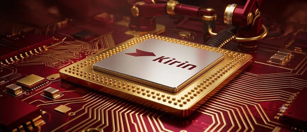
Huawei is advancing semiconductor manufacturing with the introduction of a hybrid bonding design concept slated for its Kirin 2026 chipset, signaling a significant push toward next-generation integration density.
This sophisticated approach addresses critical scaling challenges inherent in advanced logic and memory integration. The adoption of hybrid bonding promises higher interconnectivity and reduced parasitic resistance compared to traditional through-silicon via (TSV) methods.
Technical Exploration of Hybrid Bonding
The core innovation lies in the precise, direct metal-to-metal bonding between different silicon dies. This technique enables unprecedented vertical integration of heterogeneous components onto a single substrate or package structure.
For the Kirin 2026 series, Huawei intends to leverage this technology to pack more functionality into smaller footprints while simultaneously improving overall power efficiency. The design facilitates tighter coupling between compute elements and memory stacks, which is crucial for sustaining performance gains in demanding mobile applications.
The implementation requires extremely high precision in wafer thinning and surface preparation. Achieving reliable bonding at the nanometer scale necessitates stringent process control throughout the fabrication sequence. Huawei's announcement indicates a maturation of its internal process capabilities necessary to execute this complex integration methodology successfully.
This move is strategically important as it positions Kirin against competitors relying on incremental improvements in lithography alone. Hybrid bonding represents a paradigm shift toward 3D stacking architectures that fundamentally alter how chip functionality is realized.
Implications for Mobile Computing
The successful deployment of hybrid bonding within the Kirin 2026 chipset has wide-ranging implications for the high-end mobile processor market. Enhanced integration density directly translates to superior performance per watt, a key metric for flagship smartphones.
By minimizing the distance signals must travel between logic and memory layers, latency is reduced, allowing AI processing units and specialized accelerators within the Kirin chip to operate with greater throughput. This capability supports increasingly complex on-device machine learning workloads.
Furthermore, this advanced packaging technique aids in thermal management. By optimizing the physical arrangement of components, Huawei can better control heat dissipation, a persistent bottleneck in high-performance mobile System-on-Chips (SoCs).
Industry analysts view this as a decisive commitment from Huawei to lead the next wave of semiconductor innovation beyond current node scaling limits. The transition toward hybrid bonding signals a shift where packaging technology becomes as critical, if not more so, than transistor geometry in defining future chip performance.
The development timeline for Kirin 2026 suggests that these advanced fabrication techniques are moving from research prototypes into production-ready designs within the near term. As we covered in our story on Huawei Kirin 9030 Pro Chipset Delivering Massive 76% Performance Leap, this trend continues to shape the strategic landscape.