
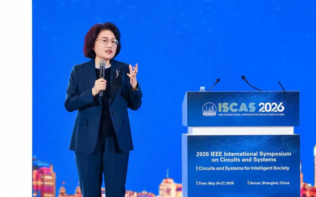
Huawei's Tau Law proposes logic folding as the necessary post-Dennard scaling pathway to achieve 1.4nm chip fabrication, fundamentally redefining how semiconductor scaling will proceed.
The Shift Beyond Traditional Scaling Limits
This novel framework addresses the physical limitations encountered when traditional Dennard scaling—where voltage and current scale proportionally with transistor size—has plateaued in advanced chip manufacturing.
Huawei asserts that continuing to rely solely on aggressive feature size reduction without architectural innovation will eventually yield diminishing returns on performance gains relative to power consumption.
The Tau Law introduces the concept of logic folding, a technique designed to pack significantly more computational density into the same physical area by restructuring transistor connections and operational logic within the chip architecture itself.
This approach moves beyond merely shrinking individual transistors; instead, it alters how those transistors interact to perform complex calculations.
Industry analysts suggest this represents a critical paradigm shift, moving semiconductor development from a purely geometric problem (how small can we make things?) to an architectural and topological one (how efficiently can we organize the logic?).
The implications for advanced computing sectors, including AI accelerators and high-performance computing, are substantial, suggesting that performance gains in the coming years may derive more from clever organization than raw lithographic shrinkage.
Logic Folding Mechanics
Technically, logic folding involves leveraging multi-level or stacked transistor arrangements not just for vertical integration but specifically to compress logical operations into tighter spatial footprints.
This methodology allows designers to implement complex functions using fewer overall transistors or by making the existing transistors perform multiple sequential roles within a single clock cycle sequence.
The projected target of 1.4nm is positioned as an achievable milestone under this new scaling model, circumventing the power density challenges that plague conventional extrapolation from current nodes like 3nm and 2nm.
The success of this scaling path hinges on overcoming intricate challenges related to interconnect resistance and thermal management within these densely folded structures.
Furthermore, Huawei’s proposal suggests that future process nodes will require much closer collaboration between hardware architects and process engineers than has historically been necessary.
The market reaction anticipates a competitive scramble among major semiconductor foundries to develop the fabrication capabilities required to implement logic folding reliably at scale.
If successfully commercialized, the Tau Law framework could dictate the roadmap for advanced silicon development well into the late 2020s and beyond, offering a viable escape route from the physical constraints of Moore's Law as traditionally understood.