
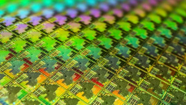
Huawei is constructing a massive 12-inch chip wafer plant to aggressively mitigate global DRAM shortages and solidify its advanced manufacturing capabilities.
Strategic Capacity Expansion
The investment signals Huawei's strategic pivot toward securing high-volume, cutting-edge semiconductor production amidst persistent supply chain volatility. This new facility represents a significant commitment to expanding domestic capacity within China, directly addressing bottlenecks in the memory chip sector that have impacted numerous global electronics manufacturers.
The construction project is engineered specifically to handle 12-inch wafers, the industry standard for producing high-density and advanced semiconductor components. Moving to a larger wafer size allows for greater yield per run and facilitates the production of more complex, high-performance integrated circuits required by next-generation consumer electronics and data infrastructure.
The impetus behind this substantial capital expenditure is twofold: mitigating immediate DRAM scarcity and establishing long-term technological self-sufficiency. Global semiconductor shortages have exposed vulnerabilities in reliance on concentrated production hubs, prompting major technology firms like Huawei to accelerate localized, large-scale fabrication projects.
This move positions Huawei not merely as a high-volume consumer of components but as a major producer capable of influencing supply dynamics. The 12-inch platform is critical because it supports leading-edge nodes necessary for advanced memory architectures and sophisticated processing units, moving beyond standard commodity chip production.
Impact on Global Semiconductor Landscape
The commissioning of this plant is anticipated to have a measurable effect on the regional and potentially global semiconductor ecosystem. By increasing its own capacity for high-quality DRAM components, Huawei can better serve its extensive internal product lines while also participating more actively in external supply chains.
Analysts suggest that such massive domestic buildouts are part of a broader, state-supported industrial policy push across China to achieve technological independence from international dependencies. For Huawei, this translates directly into enhanced control over the design-to-delivery cycle for its flagship devices and enterprise solutions.
The construction timeline indicates an aggressive deployment schedule, underscoring the urgency with which Huawei perceives the need to stabilize input costs and guarantee component availability. The transition to 12-inch manufacturing is not trivial; it requires substantial investment in photolithography equipment, cleanroom environments, and highly specialized process engineering expertise.
This strategic move underscores a maturation of Huawei's semiconductor ambitions, shifting focus from merely assembling components using external suppliers to controlling the fabrication process itself. The successful operation of this 12-inch wafer plant will serve as a critical benchmark for its technological prowess in the increasingly competitive global chip manufacturing arena.