
🎙 Listen to a summary of this story
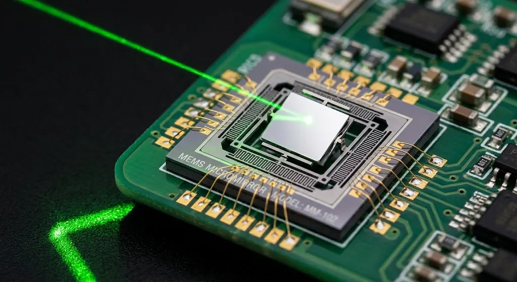
Suzhou Chipsens has introduced a sophisticated MEMS micromirror array chip, advancing optical circuit switching capabilities crucial for the next generation of high-speed data center networking.
The new chip utilizes Micro-Electro-Mechanical Systems (MEMS) technology to create highly efficient optical switching elements, directly addressing the growing bandwidth demands within massive cloud infrastructure and telecommunication backbones. This development positions the company at the forefront of silicon photonics integration.
Optical Circuit Switching (OCS) represents a fundamental shift from traditional electronic routing, allowing for instantaneous, low-latency path creation across optical networks. By employing MEMS micromirrors, Suzhou Chipsens achieves high switching density and low power consumption, characteristics essential for the energy-constrained environments of hyperscale data centers.
The architectural advantage of this micromirror array lies in its ability to precisely steer light beams across a planar substrate. This physical manipulation of light enables the creation of complex, reconfigurable optical paths without the need for intermediate electrical conversion stages, which typically introduce significant latency and power overhead.
Technically, the array demonstrates high optical throughput while maintaining sub-nanosecond switching times. The integration methodology allows for seamless compatibility with existing photonic integration platforms, lowering the barrier to adoption for major network equipment manufacturers seeking to upgrade their switching fabric.
The strategic importance of this technology cannot be overstated in the context of expanding data traffic. As data volumes continue to scale exponentially, the bottleneck often shifts from raw optical transmission capacity to the efficiency and speed of the switching apparatus controlling that capacity.
Technical Specifications and Market Implications
This micromirror array chip is engineered to operate within demanding operational parameters, providing robust performance under continuous load. Its design minimizes optical insertion loss, ensuring that the signal integrity remains high even when multiple switching operations are performed concurrently within the array.
The market implications are substantial, particularly for service providers and cloud computing entities grappling with traffic burstiness and the need for dynamic resource allocation. Traditional optical switches, while effective, often suffer from size and power constraints that become prohibitive at petabit-scale operations.
By leveraging MEMS, Suzhou Chipsens provides a scalable solution that reduces the overall footprint of optical switching hardware. This density gain translates directly into lower capital expenditure for network operators building out new core infrastructure.
The company's focus on this specific application—OCS—highlights a strategic pivot toward specialized optical components rather than generalized photonic ICs. This targeted approach allows for deeper optimization tailored precisely to the stringent requirements of high-performance networking applications.
Industry analysts suggest that the maturation of MEMS-based optical switching is a critical enabler for realizing the full potential of 800G and beyond transmission rates. The chip serves as a vital component in constructing coherent optical networks capable of handling future traffic demands.
Suzhou Chipsens continues to solidify its position in the advanced semiconductor landscape by delivering high-performance, specialized optical solutions that directly impact the efficiency and scalability of global digital communication networks.